Daily Current Affairs : 14-August-2024
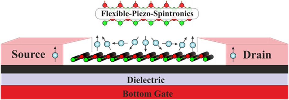
Researchers at the Institute of Nano Science and Technology (INST) in India have made an exciting leap forward in the field of spintronics, which could revolutionize the future of electronics and quantum computing. The team has developed a transparent layer between two insulating materials, enabling the movement of electrons in a two-dimensional plane at room temperature, with their spins aligned. This discovery opens up several possibilities for faster, more energy-efficient devices in various fields, from quantum computing to data storage.
What is Spintronics?
Spintronics is a cutting-edge area of research focused on utilizing the spin of electrons, in addition to their electric charge, to store and process information. By manipulating electron spins, researchers can create faster, smaller, and more efficient electronic devices. This technology has the potential to reduce energy consumption and increase the speed of devices, making it a crucial area for the future of electronics.
The Key Discovery: Two-Dimensional Electron Gas
In this research, the INST team created a two-dimensional electron gas (2DEG) at the interface of two materials: LaFeO3 and SrTiO3. This 2DEG exhibited unique properties, which include:
- Negative Magnetoresistance: This means that the material’s resistance decreases when exposed to a magnetic field.
- Anomalous Hall Effect: This phenomenon is related to the behavior of electrons in the material under magnetic fields, leading to more efficient information processing.
Potential Applications
These unique properties of the 2DEG could lead to several exciting developments, including:
- Ultrafast, Low-Power Electronics: The ability to control electron spins at room temperature will enable the creation of faster and more energy-efficient devices.
- Quantum Devices and Data Storage: This breakthrough may pave the way for new quantum devices with enhanced functionalities, offering more powerful data storage and processing capabilities.
- Transparent Spintronic Devices: The transparent nature of the layer could be used to create spintronic devices that could be integrated into everyday items like displays or solar cells.

Important Points:
- Breakthrough in Spintronics: Researchers at the Institute of Nano Science and Technology (INST), India, have developed a transparent layer between two insulating materials that allows electron movement with aligned spins at room temperature.
- Spintronics Technology: Spintronics manipulates the spin of electrons, in addition to their charge, to enhance the performance of electronic devices, making them faster and more energy-efficient.
- Two-Dimensional Electron Gas (2DEG): The research team created a 2DEG at the interface of two materials, LaFeO3 and SrTiO3, which exhibited unique properties:
- Negative Magnetoresistance: Resistance decreases when exposed to a magnetic field.
- Anomalous Hall Effect: Improves the efficiency of information processing under magnetic fields.
- Potential Applications:
- Ultrafast, Low-Power Electronics: Controlling electron spins at room temperature can lead to the creation of faster, energy-efficient devices.
- Quantum Devices and Data Storage: The research opens possibilities for more powerful and efficient quantum devices and data storage solutions.
- Transparent Spintronic Devices: The transparent layer can be used for creating devices like displays and solar cells.
- Significance: This advancement is a major step toward developing next-generation electronics and quantum devices, driving progress in areas like quantum computing and data storage.
Why In News
Researchers at the Institute of Nano Science and Technology (INST) in India have developed a groundbreaking transparent layer between two insulating materials, enabling the movement of electrons in a two-dimensional plane at room temperature with their spins aligned. This innovative discovery paves the way for new spintronic devices that could operate at much higher speeds and lower power consumption compared to traditional electronics.
MCQs about Spintronics
-
What is the primary focus of the research conducted at the Institute of Nano Science and Technology (INST)?
A. Developing faster processors
B. Creating a transparent layer to enable electron movement
C. Enhancing battery life in devices
D. Discovering new types of materials for insulation
-
What property of the 2DEG (Two-Dimensional Electron Gas) was observed in the research?
A. Increased electrical resistance
B. Negative magnetoresistance
C. Higher power consumption
D. High thermal conductivity
-
What potential applications could arise from this groundbreaking spintronic research?
A. Development of energy storage systems
B. Creation of ultrafast, low-power electronics
C. Improvements in solar panel efficiency
D. Expansion of traditional semiconductor manufacturing
-
What unique characteristic does the newly developed material allow for in electronic devices?
A. The use of two-dimensional electron gas at low temperatures
B. The integration of spintronic devices into everyday items like displays
C. Increased use of rare earth elements in electronic components
D. The ability to use electron charge instead of spin for data storage
Boost up your confidence by appearing our Weekly Current Affairs Multiple Choice Questions
![]()


